


Yangtze River Daily Wuhan client April 14 news (reporter Li Qin correspondent Zhang Xifor) investment of 12 billion yuan pilot thin material project, from the official signing to the actual start, but 4 months; Not far away, the advanced Wuhan base of Changfei has entered the final stage of equipment commissioning, and is expected to achieve mass production in May this year.
Since the first Jiufengshan Forum was held, Optics Valley announced to build a global compound semiconductor innovation beacon and industrial highland, just two years ago, Changfei advanced, pilot thin materials and other projects of 10 billion have been launched, Tiangong core measurement, Yi Tianuo and other supporting projects rushed to the ground, covering an area of 10 square kilometers Jiufengshan Science and Technology Park, with Jiufengshan Laboratory as the innovation pole. Optical Valley compound semiconductor industry from “blooming on the point” to “on the chain into the scene”.
Another year of spring grass green, April 23 to 25, the 2025 Jiufengshan Forum and Compound Semiconductor Industry Expo (hereinafter referred to as “Jiufengshan Forum”) jointly sponsored by the third generation semiconductor industry technology innovation Strategic Alliance and Jiufengshan Laboratory will be held in Optics Valley again, and the “big coffee” of industry, university and research will gather to discuss the future of compound semiconductor innovation.
“Today’s Jiufengshan Forum is like a spark – we look forward to it igniting a global wildfire of compound semiconductor innovation!” At the recent press conference held in China’s Optical Valley Press conference Hall, the relevant person in charge of Donghu High-tech Zone invited the world to take the Jiufengshan Forum as a new starting point to jointly witness the “Optical Valley acceleration” of compound semiconductors!
Key technologies have made breakthroughs, and the “innovation ecosystem” of Jiufengshan Laboratory has developed vigorously
From materials, design, manufacturing to packaging and testing, the compound semiconductor industry is a typical technology-intensive industry, and the height of innovation determines the height of the industry.
Taking the important substrate market in the compound semiconductor industry chain as an example, international research institutions predict that the compound semiconductor substrate market will grow at a compound annual growth rate (CAGR) of 17% and will reach $3.3 billion by 2029. Analysts at YoleGroup pointed out that the compound semiconductor industry is at a critical juncture in the transition to large-diameter substrates.
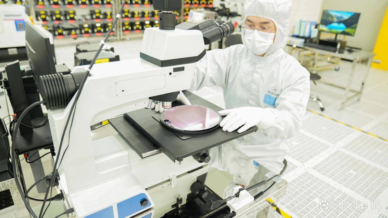
Last month, Jiufeng Mountain Laboratory announced that the world’s first 8-inch silicon-based nitrogen polar gallium nitride substrate, to ensure the high performance of gallium nitride, but also the low cost of silicon, “so that scientific research institutes, enterprises are affordable.”

Jiufengshan Laboratory 8-inch silicon-based nitrogen polar gallium nitride substrate. Correspondent for the picture
Making semiconductors is like building a house, and the substrate is the foundation of the house. The larger the diameter of a compound semiconductor substrate, the greater the number of chips that can be manufactured on a single substrate, and the lower the cost of manufacturing a unit chip. Due to the bottleneck constraints such as harsh material growth conditions and highly complex processes, there are only a few institutions in the world that can produce 2 to 4 inches of nitrogen polar gallium nitride high electron mobility substrate materials in small quantities, and the cost is very high.
This breakthrough of Jiufengshan Laboratory not only breaks the international technology monopoly, but also provides strong technical support for the improvement of system-level chips such as radio frequency front-end in terms of frequency, efficiency and integration, and will promote the rapid development of cutting-edge technologies such as next-generation communication, automatic driving, radar detection and microwave energy transmission.
“Picked out a few hard bones in a row.” At the media meeting held in Jiu-Fengshan Laboratory, Wu Chang, chief expert in the wireless field of Jiu-Fengshan Laboratory Research Center, introduced that the laboratory has advanced the layout of gallium nitride materials as the core of research at the beginning of its establishment, and has now achieved a series of breakthrough achievements from materials, devices to industrial applications in an all-round way.
Back in April 2023, Jiufengshan Laboratory was officially put into operation, and Optics Valley established a leading compound semiconductor research and development and innovation center. As one of the top ten laboratories in Hubei Province, Jiufengshan Laboratory focuses on the research and development and innovation of compound semiconductors, focuses on tackling the “stuck neck” problem, and successively achieved the world’s first 8-inch silicon light film lithium niobate photoelectric integrated wafer, heterogeneous integrated “chip light” and other “milestone” achievements.
With the continuous breakthrough of key technologies, the blocked points, stuck points and breakpoints of the industrial chain have been opened up, and the “innovation ecosystem” of Jiufengshan Laboratory is also booming. So far, it has attracted more than 500 enterprises and scientific research institutions to seek cooperation, more than 30 enterprises live in close proximity, and more and more innovative achievements have come out of the Optical Valley.
Together with Jiufengshan Laboratory, Huagong Technology developed the first set of high-end semiconductor wafer laser cutting series equipment, a number of key indicators first in the country; Yitenuo successfully delivered the first set of high-power wafer sealing equipment in China, and the core components were 100% self-developed.
Major projects are coming, Optics Valley Lights Compound semiconductor “lighthouse of the world”
On April 9, the project site of the pilot thin material high-end compound semiconductor materials and chip industrialization base in the East Lake Comprehensive protection Zone was filled with mechanical roar.
Lead Technology Group, headquartered in Guangzhou, is the world’s leading sparse metal enterprise, and is the first manufacturer in China to realize 8-inch gallium arsenide substrate and 6-inch indium phosphide substrate. The shipments of gallium arsenide rank first in China and top three in the world. After the completion of the project with a planned investment of 12 billion yuan, it will effectively fill the gap in semiconductor substrates and epitaxial materials required by optical Valley optical communication and laser industry.
“This is not only a research and development and production base, but also the central China headquarters.” Project leader Xiong Wei frequent travel between Guangzhou and Optics Valley, in his view, Wuhan nine provinces, both science and education town, but also has the advantage of industrial agglomeration, “communication with customers, recruitment of talent are very convenient.”
It is understood that the project has been fully capped, while recruiting talents while designing production lines, and plans to achieve partial production before the end of the year. Xiong Wei sighed, from the signing in March 2024, to the actual start in July of the same year, and then to the sprint cap in January this year, “such a large project and such a fast construction speed are very difficult.”
Also witnessing the construction of 10 billion projects “Optical Valley speed”, there is the advanced Wuhan base of Changfei not far away.
From the first pile to the structural capping, the construction of the advanced factory took less than 10 months, and the first fab process equipment was moved in at the end of last year. “In less than a year and a half, we started from a wasteland and built the largest silicon carbide chip production base in China.” Chen Zhongguo, president of Changfei Advanced, said that the Wuhan base has entered the final stage of equipment commissioning and is expected to achieve mass production next month.
The first Jiufengshan Forum was held two years ago. At the opening ceremony, focusing on building a global compound semiconductor innovation beacon and industrial highland, Optics Valley released the Jiufengshan Science and Technology Park plan, established an industrial fund, and signed projects with a total amount of nearly 30 billion yuan.

2024 Jiufengshan Forum has attracted the attention of the industry.
With Jiufengshan Forum as the vanguard, upstream and downstream companies of compound semiconductors gather in optical Valley. Only in a investment meeting more than 10 days ago, there are 10 pan-semiconductor projects signed to settle in Optical Valley, covering the “chip design – wafer manufacturing – packaging and testing – equipment materials” industrial chain.
Separated from the Jiufengshan Laboratory all the way, the Jiufengshan Science and Technology Park, covering an area of 10 square kilometers, has been outlined. It is understood that the park side construction side investment, has been fully booked.
“Optical Valley compound semiconductor industry ecological accumulation, comprehensive momentum, with Jiufengshan Laboratory as the innovation pole core, ran out of a remarkable ‘acceleration’.” The person in charge of the East Lake high-tech zone said at a press conference.
According to reports, in the next step, Optics Valley will launch a special support policy for third-generation semiconductors, build a compound semiconductor Academy and incubation acceleration base, build a compound semiconductor industry innovation block, and become a “world lighthouse” in the field of compound semiconductors.
Leading enterprises, industry-university-research cooperation sing the “assembly signal”
As a semiconductor material composed of two or more elements, compound semiconductors have become the core materials for independent innovation, development and transformation and upgrading of optoelectronics, wireless communication and power electronics industries with their excellent performance, and are regarded as opportunities for lane overtaking in China’s semiconductor industry.
“This is a historically critical period for the reshaping of the global semiconductor landscape.” At the Jiufengshan Forum last year, Wu Ling, chairman of the third-generation semiconductor industry technology Innovation Strategic Alliance, stressed that the compound semiconductor industry is an important breakthrough in the process of restructuring the global semiconductor industry competition pattern, “solve the breakpoints and blocking points, open up the industrial chain, and enter the world’s advanced ranks with 10 years of the whole chain.”
This year’s Jiufengshan Forum for the first time to achieve the three-dimensional linkage of science and technology, industry and culture, in addition to nearly 200 keynote speeches in 3 days, more than 200 leading enterprises and industry new exhibitors from more than 10 countries and regions were invited to participate in the exhibition, covering the whole industry chain of materials, design, equipment, manufacturing and terminal applications, and the scale has doubled compared with last year.